THE ORIGIN OF AUDIBLE DIFFERENCIES IN THE QUALITY OF
RADIOTRANSMISSION OF THE AMPLIFIERS OF SOUND FREQUENCIES
A.M. Likhnitsky
All-state scientific institute of radio and acoustics named
after A.S. Popov
The entire history of the development of
transistors used for amplification of sound can be divided into three periods.
During the first period the sound produced through the transistor amplifiers of
sound frequency (ASF) seemed attractive, bright, and free of distortions.
Unlike lamp amplifiers, the transistor ASF showed unbounded amplitude-frequency
characteristics (AFC). The popularity of a “transistor sound” lasted until mid
60-ies. After that, the transistor sound gradually became a synonym for
somewhat unpleasant in terms of subjective sensations, though the objective
parameters of transistor ASF formally kept on passing the requirements of
undistorted audio transmission. The phenomenon of unobserved audible
distortions turned out to be the reason for the appearance of the term
“mystical concepts” [1] in technical literature, where transistor was
considered to be the factor responsible for the deterioration of sound. And it
has just happened recently when this point of view shifted towards the very
much different one, where the uncontrolled subjective distortions were
considered the true reason for unpleasant subjective sensations.
The search for distortions most sensible
to ear was initiated in the early 70-ies by a number of companies –
manufacturers of ASF [1,2]. In particular, it was established [2] that among a
large number of descriptive definitions, used by experts for the evaluation of
quality of audio transmission of ASF, one can identify two groups: the first
one may be described by the ”opacity,” “stiffness,” “metalicity,”
“annoyance” of sound; the second one comprises the dullness of bass, frequency
and time fuzziness, the loss of sharpness.
The first group is controlled by the
effects of perception of non-linear distortions and their resultants of higher
order, beats in particular. These distortions form the so-called “left” with
respect to the signal, and therefore, not masked distortion spectrum. The
second group turned out to be a mystery concerning what sensations should be
attributed to what type of objective distortions. While performing subjective
expertise of electrical recording devices, Moller [3]
observed the sensations, which were the most similar to those mentioned above.
He presumed that those sensations might be correlated to the Bass
Intermodulation (BIM). Moller defined BIM as a
parasite modulation of the useful signal by its distortions in the spectral
range between 2 and 60 Hz. Let’s define the signal modulation by the amplitude
as BIMA and by frequency as BIMF.
Why should BIM be considered as the most
important parameter that characterizes the distortions of the audio recording
equipment? First, the resultants of BIM coincide with the components of the
useful signal that reflect the emotional context of voice and music [4].
Second, the spectrum of BIM distortions lies within the range of critical
audibility band, and, therefore, falls within the range of maximum sensitivity
to the difference between the frequency and amplitude modulation of signal [5].
In spite of the significance of BIM
distortions for the quality of audio transmission, they have not been
controlled in ASF. This is a result of the absence of the physical concept, which
could explain the formation of BIM. Note, that BIM distortions (known as the
detonation of sound[1])
are easily explained by oscillations of linear velocity of the sound recording
material [6] and have been controlled in the recording devices for quite a long
time.
We assumed that transistor ASF produces
audible “sound detonation.” In order to prove this supposition, the detonation
coefficient of several hi-fi transistor ASF was measured in the regime of
signal addition of two sine signals on 20 and 3,150 Hz with the amplitude ratio
4:1 at the input of these ASF. The results unexpectedly gave us the value of
the detonation coefficient equal to 0.6% when measured with the standard
flutter meter, provided that the ASF has a nominal output voltage. This value
of the detonation coefficient 10 times [7] exceeds the noticeability
threshold for this type of distortions, and 2 times exceeds the tolerance value
for these distortions in the C-class tape recorders [8]. Here we set forward
the physical concept for appearance of BIM distortions in ASF built on bipolar
transistors.
It is known [9,10] that the temperature
increase at the p-n junction of bipolar transistor is accompanied by the
increase of the current gain from 0.3%/K to 0.5%/K and the decrease of the base-emitter
voltage at 2.2mV/K. The thermal sensitivity of these parameters has been
accounted for earlier from the position of providing the thermal stability for
the operating point of the amplification stage [11]. Paul [12] pointed out that
the temperature oscillations at the p-n junction, produced by the oscillation
of the dissipated power on the collector, affect the transforming properties of
transistors. He gave the name Mitlaufeffekt
(non-isothermal effect) to this effect. However, the formation of these
distortions, caused by the thermoelectric mechanism of signal transformation in
ASF, was for the first time addressed by Opperman
[13]. This communication didn’t raise much interest among professionals, since
it lacked the quantitative estimations for the observed distortions. Later, Fishtain [14] noticed the end-to-end phase shifts in the
infrasound region at the differential stage built on bipolar transistors. Those
shifts lied within the frequency region where the inertia of electrical
processes shouldn’t play any role. The infrasound region distortions were
explained by the influence of the AC component of p-n junction temperature on
the thermosensitive parameters of bipolar
transistors. However, the connection between BIM distortion in ASF and temperature-caused
distortions was not demonstrated in any of the publications, to the best
knowledge of the author. Due to the obscurity of the reasons for BIM
appearance, we have studied the physical processes responsible for the
formation of linear and non-linear distortions in typical 3-stage transistor
ASF. As a result, it was proved [15] that thermal distortions are being formed
not only in separate stages, but practically in all transistor sub-circuits in
typical ASF. The most significant of the obtained results was the establishment
of the connection between thermal distortions and formation of BIM distortions.
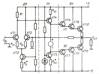
Fig.1. The principle electrical circuit of
a typical ASF built on bipolar transistors[2].
The study of the conditions for the appearance
of thermal distortions was conducted in ASF, according to Fig.1, where the
output stage (OS) (transistors VT6 – VT11) comprises three Darlington-type
class B emitter-followers. The driver stage (DR) (transistor VT4) is built as a
common emitter, where the collector circuit has a dynamic load (DL) (transistor
VT5). The differential stage (DS) (transistors VT1, VT2) is completed according
to the asymmetrical circuit with a dynamical load (transistor VT3) in the
emitter circuit.
Thermal distortions in
the output stage.
Any change in the amplitude of the voice
or musical signal is accompanied by the temporal change of the p-n junction
temperature of OS transistors. This is clear if one recognizes that for B-class
OS stage the average power dissipated on the collector of the output stage
transistors during one period of the amplified signal is a function of the
amplitude of that signal [16]:
![]()
where Um3 is the amplitude of
the signal at the output of ASF in Volts, E is the source voltage of the OS leg
in Volts, and RH3 is the OS load resistance in Ohms.
Though the rate of change of p-n junction
temperature of OS transistors is limited by the inertia of thermoelectric
transformation, the value of the thermal time constant junction-case is not
sufficient for smoothing out the gradually changing instantaneous power on the
collector of OS transistors. When the dissipated power at the collector of OS
transistor has a maximum value, the instantaneous p-n junction temperature
could possibly reach its maximum allowed value 150°C, and during the intervals
of the absence of signal the temperature can decrease to the temperature of the
transistor case [15].
The maximum operating temperature of the
OS transistor case is 60-70°C, which is preset during the fabrication of ASF
[17]. This value tends to be a compromise between the effective heat transfer
away from the output transistors and maintaining of the strict requirements to
the standards of massive ASF. It can be concluded that the optimally designed
ASF can reveal 80-90°C difference in the values of the instantaneous p-n
junction temperature of OS transistors of B-class ASF.
In order to quantitatively estimate the
influence of AC component of the p-n junction temperature on distortions, we
will have to find some relative increase in current gain of the transistors.
Let’s use the value of the temperature jump across the p-n junction and the
dependence of current gain on temperature [9] that was determined earlier. It
can be shown that the change of gain can be as high as 50% for each transistor
in OS, and as high as 300% for the circuit of 3 transistors in OS. Taking into
account all said above, the voltage gain for OS is:
m3
= RH3 / (RH3
+ R3); R3 = R2 / (β1 + 1)( β 2 + 1)( β 3 + 1) (1)
where R2, R3 are the output resistance of
DS and OS, respectively, in Ohms; β 1, β 2, β 3 are the current gains of OS transistors
of the emitter-follower connected in series. The output resistance of the
emitter-follower circuit is variable, due to change of the current gain of the
OS transistors, whereas the relative change of the value of R3 can
be as high as 3. According to (1), the change in the value of R3 is
the reason for the instability of the current gain μ3. This shows itself as a parasite
amplitude modulation of the useful signal at OS output by the envelope of the
same signal. The experts from “Sansui” [18] named this type of distortions as
“envelope distortions,” although those distortions rather belong to the BIMA
type due to their spectral characteristics. These distortions are observed only
for non-stationary signal at the input of ASF, and therefore cannot be detected
by the traditional methods used to measure intermodulation distortions. One of
the effective methods for the “envelope distortion” control is the response of
OS to the amplitude-modulated signal or a pitch burst [18]. In the latter case
the relative change of the amplitude of the pitch burst at the output of OS
(during the first 100 ms from its initiation) can be considered as a measure of
the envelope distortion. The magnitude of the envelope distortion for OS as an
emitter-follower (Fig.1) can be written as:
![]()
where we have used the
voltage gain of OS, defined according to (1) at the maximum and the minimum
temperature of p-n junction. In case of the typical values of R2 > RH3(β 1 + 1)( β 2 + 1)( β 3 + 1) for OS control from the current source,
these envelope distortions can be as high as 300%. If the opposite inequality
is being held (OS is controlled by the voltage source), the thermal sensitivity
of the current gain can be neglected. The driver stage DR (see Fig.1) built on
the bipolar transistor VT4 operates in the regime A as a common-collector
amplifier. The thermal distortions in DR are formed when the instantaneous
temperature of p-n junction of VT4 changes due to oscillations of the
dissipated power on its collector. This power dissipation can be calculated for
operating points of VT4, where the AC component of this dissipated power can be
represented as:
![]() ,
,
where UП2 is the source voltage
for DS, UO2 is the collector-emitter voltage when the signal with
the instantaneous value of uk is
not present, ![]() is the load resistance in the collector leg.
is the load resistance in the collector leg.
Since DS operates in the regime of
powering the input from the voltage source, it turns out that the thermal
sensitivity of p-n junction base-emitter voltage for VT4 becomes quite
significant. This voltage causes the creation of the unaccounted feedback
coupling between collector and base-emitter circuit [15]. The feedback coupling
(FC) circuit includes the transformation of AC voltage U2 into
instantaneously dissipated power Pk(t), followed by
the change in p-n junction temperature and then by the instantaneous change of
the base-emitter voltage with the coefficient – 2.2 mV/K. This thermoelectric
feedback coupling (TEFC) in transistor VT4 is very much similar to the
electromechanical one. The expression for the transfer characteristic of TEFC
circuit of DR can be written in the operational form as [15]:
![]()
where RT2 and tП-К are the thermal resistance, in
Kelvin/Watt, and the thermal time constant of the junction-case of transistor
VT4, in sec, respectively; Pk(s) – is the AC component of the instantaneous power
dissipated on the collector of that transistor written in the operational form,
in Watts; U2(s) is the AC component of the voltage at the output of
DR in the operational form, in Volts. This characteristic exhibits inertial
non-linearity of the second order.
The transfer characteristic of the closed
system with the inertial non-linear FC can be represented in a simplified form
[19] as a product of the frequency-dependent function of the linear part H2(s)
and non-linear transfer function F2 (u2) with the
resistive character. As consequence, we get [15]:
![]()
where ![]() is the resistance in the emitter leg of VT4, in Ohms;
is the resistance in the emitter leg of VT4, in Ohms; ![]() is
the time constant that corresponds to the pole frequency of the transfer
function of DR, in sec. This function can be determined using the following
condition:
is
the time constant that corresponds to the pole frequency of the transfer
function of DR, in sec. This function can be determined using the following
condition:
![]()
where ![]() - is
the voltage gain of DR without TEFC.
- is
the voltage gain of DR without TEFC.
From the expression (3):
![]()
For the values ![]() of the frequency, i.e. at
of the frequency, i.e. at![]() ,
the dependencies of AFC and non-linear distortions of DR (see Fig.2) has been
obtained [15]. It is seen from the figure that the influence of TEFC ceases
above the frequency
,
the dependencies of AFC and non-linear distortions of DR (see Fig.2) has been
obtained [15]. It is seen from the figure that the influence of TEFC ceases
above the frequency ![]() , the AFC of the DR stage becomes flat,
and the non-linear distortions die with the rate of 6 dB/oct.
If
, the AFC of the DR stage becomes flat,
and the non-linear distortions die with the rate of 6 dB/oct.
If ![]() in the equation (2), and if Um2
< Un2 ~ Uo2 (Um2 is the amplitude of the AC
component of the voltage at the output of DR), then the value of the
coefficient of the second harmonic of DR is given by the formula [15]:
in the equation (2), and if Um2
< Un2 ~ Uo2 (Um2 is the amplitude of the AC
component of the voltage at the output of DR), then the value of the
coefficient of the second harmonic of DR is given by the formula [15]:
![]()
One important feature of TEFC in DR is the
instability of the pole frequency полюса ![]() at u2>0. In other words,
this frequency has a deviation with the relative magnitude:
at u2>0. In other words,
this frequency has a deviation with the relative magnitude:
![]()
This means that the useful signal (with
the frequency ![]() ) at
the output of DR is phase-modulated by the interfering signal with the
frequency
) at
the output of DR is phase-modulated by the interfering signal with the
frequency ![]() if the two of them are simultaneously
present at the input of DR, where the useful signal has frequency
if the two of them are simultaneously
present at the input of DR, where the useful signal has frequency ![]() , and the interfering signal (infrasound)
has a frequency
, and the interfering signal (infrasound)
has a frequency ![]() and the amplitude larger than that of the
useful signal. The phase deviation in this case equals:
and the amplitude larger than that of the
useful signal. The phase deviation in this case equals:
![]()
According to the known relationship [20]:
![]() ,
,
the phase deviation represents itself as a
detonation of the useful signal, i.e. the BIM distortions appear at the
frequency close to the pole frequency ![]() as result of infrasound oscillations at
the input of ASF in DR.
as result of infrasound oscillations at
the input of ASF in DR.
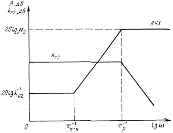
Fig.2. Dependence of distortions (AFC and
non-linear) on frequency in the driver stage (DR) of ASF.
Calculation of distortions in DR.
As an example, let us calculate the range
of frequencies and amplification roll-off, as well as the second harmonic
coefficient and BIM distortions caused by TEFC in DR. For this example we will
take the values relevant for the transistor KT602Б, which has RT=45 K/W [21] and ![]() = 6 ms. The transistor mode in DR is the
following:
= 6 ms. The transistor mode in DR is the
following:
Uo= 20 V, Un= 125 V, Rn= 15 kOhm, Ie = 7 mA, Re=
4.3 Ohm (at the average p-n junction temperature), Um= 15 V. Using
these parameters (equations (2), (3), (5), and (6)-(8)), the calculation yields
the following values [15]:
·
Relative amplification roll-off at low frequency ![]() d=3.24 (10dB);
d=3.24 (10dB);
·
The frequency where the amplification decay starts (at
the level –3 dB) fp = 86 Hz;
·
The frequency where the amplification decay stops (at
the level +3 dB)![]() = 26.3 Hz;
= 26.3 Hz;
·
Harmonic distortions at ![]() = 11.7%;
= 11.7%;
·
The relative deviation of the pole frequency fp equals 10.3%; the deviation of the phase of
the signal for the frequency in the vicinity of the pole frequency is 0.053 rad, which corresponds to the 1.3% of the frequency
detonation.
·
Thermal distortions in the differential stage.
The observation of the thermal distortions
in DR (see Fig.1) motivated us to study TEFC in the transistors VT1, VT2 of the
differential stage DS [15], although the low output voltage of DS and
insignificant power dissipated on the collector of its transistors do not
create any conditions for sufficient impact of TEFC. The attributes of TEFC in
DS are the following:
·
The voltage at the output of DS is negligibly small
(approximately 1000 times smaller than at the output of DR), therefore, the
transfer characteristic of TEFC in DS can be assumed linear;
·
TEFC in DS has a sign opposite to that of TEFC in DR,
since the source voltage of DS and collector-emitter voltage of transistors in
DS are approximately equal;
·
The signals at the output of TEFC in VT1 and VT2 are
added together, since they are connected between the emitters of those
transistors in series and in phase.
Based on the statements above, the
transfer function of DS can be written as [15]:
where ![]() is the voltage transfer coefficient of DS (without the
influence of TEFC);
is the voltage transfer coefficient of DS (without the
influence of TEFC);
![]() 01(s) is the transfer characteristic of
TEFC in DS;
01(s) is the transfer characteristic of
TEFC in DS; ![]() is the thermal time constant of
junction-case of the transistors VT1, VT2, in sec;
is the thermal time constant of
junction-case of the transistors VT1, VT2, in sec; ![]() is the time constant corresponding to the
pole frequency of the transfer function of DS with TEFC (is defined similar as
is the time constant corresponding to the
pole frequency of the transfer function of DS with TEFC (is defined similar as![]() , see the equation (4)), in sec;
, see the equation (4)), in sec; ![]() are
the resistance of the DS load and the emitter of VT1, VT2, respectively (see
Fig.1), in Ohms; RT1 is the thermal resistance of the junction-case
of the transistors VT1, VT2, in K/W; U01 is the collector-emitter
voltage of transistor VT1, in Volts.
are
the resistance of the DS load and the emitter of VT1, VT2, respectively (see
Fig.1), in Ohms; RT1 is the thermal resistance of the junction-case
of the transistors VT1, VT2, in K/W; U01 is the collector-emitter
voltage of transistor VT1, in Volts.
In practical embodiments of DS circuits
the following inequality holds: ![]() . Hence, TEFC is positive. Given that
. Hence, TEFC is positive. Given that ![]() , it means that the instability of the DS
regime takes place at the frequency close to zero. This instability can be
excluded if the condition
, it means that the instability of the DS
regime takes place at the frequency close to zero. This instability can be
excluded if the condition ![]() or 2.2
or 2.2![]() is satisfied, where R
is satisfied, where R![]() is the thermal resistance of p-n
junction-case of transistors VT1 and VT2 of DS, in K/W.
is the thermal resistance of p-n
junction-case of transistors VT1 and VT2 of DS, in K/W.
Thereby, substantial linear distortions
appear in DS in the infrasound frequency region. They show themselves as a
leading shift of the signal phase, and also in the boost of AFC. This boost is
limited, since the operational point also shifts into the region of TEFC
conditional stability. Similar results were obtained in [14].
Thermal distortions in the dynamical load.
The collector circuit of transistor VT4 of
DR and emitter circuit of transistors VT1, VT2 of DS (see Fig.1) comprises the
dynamical load (DL) built on the bipolar transistor. The external circuit of
the base of that bipolar transistor has a relatively small resistance. As a
result of it, the influence of TEFC is considerable in DL (like in DS and DR).
Since DL is a two-terminal device, the TEFC appears as a change in the
total dynamic resistance of DL in the low-frequency sound region. In this case
TEFC can be calculated as being connected in series by voltage.
The dependence of the total dynamic resistance
of DL on the parameters of the sub-circuit can be written as:
![]()
where ![]() is the dynamical resistance of DL (without
the influence of TEFC), in Ohms;
is the dynamical resistance of DL (without
the influence of TEFC), in Ohms; ![]() * is
the transfer characteristic of TEFC in DL; RK is the resistance of
all circuits parallel to DL (including self) without any influence of TEFC, in
Ohms; R*Э is the resistance in the emitter circuit
of DL, in Ohms.
* is
the transfer characteristic of TEFC in DL; RK is the resistance of
all circuits parallel to DL (including self) without any influence of TEFC, in
Ohms; R*Э is the resistance in the emitter circuit
of DL, in Ohms.
When DL is included in DS, i.e. in the
legs of the transistors VT1, VT2, DS behaves similar to a linear two-terminal device.
This can be explained by the insufficiency of in-phase part of the signal
applied to DL. Although DL is not a source of the non-linear distortions in DS,
the change in the value of the dynamical resistance of the former contributes
to the in-phase part of the signal at the output of ASF. Consequently, it will
signify the appearance of other types of distortions [9] when ASF operates in
the negative feedback regime.
The decrease of the total dynamic
resistance of DL, built on transistor VT5, has a different effect on the
operation of DR. As it has been shown in [15], the low-signal transfer function
of DR (with DL) can be written as:
where ![]() is the thermal time constant junction-case
of the transistor VT5, in K/W;
is the thermal time constant junction-case
of the transistor VT5, in K/W; ![]() is the time constant corresponding to the pole
frequency of the fall of amplification of DR due to TEFC in DL (is determined
similar as
is the time constant corresponding to the pole
frequency of the fall of amplification of DR due to TEFC in DL (is determined
similar as ![]() , see equation (4)), in sec; RK2
is the resistance of all legs connected in parallel to the output of DR,
including the dynamic resistance of collector of VT4 (without TEFC), in Ohms;
, see equation (4)), in sec; RK2
is the resistance of all legs connected in parallel to the output of DR,
including the dynamic resistance of collector of VT4 (without TEFC), in Ohms; ![]() is the thermal resistance of the junction-case of the
transistor VT5, in K/W;
is the thermal resistance of the junction-case of the
transistor VT5, in K/W; ![]()
![]() are
the voltage source of DL (extrapolated value) and the collector-emitter voltage
of the transistor VT5 (without a signal), respectively, in Volts;
are
the voltage source of DL (extrapolated value) and the collector-emitter voltage
of the transistor VT5 (without a signal), respectively, in Volts; ![]() is the resistance in the emitter circuit
of VT5, in Ohms.
is the resistance in the emitter circuit
of VT5, in Ohms.
It is important to notice that the
employment of DL in DR ensures the partial linearization of the stage because
of mutual compensation of the higher-order terms, due to TEFC in both VT4 and
VT5.
Thermal distortions in
the amplifier with the common negative feedback coupling.
The discussed thermal distortions in DS,
DR and OS are being observed as various non-linear distortions of the signal at
the output of ASF, connected in a common negative feedback coupling.
Harmonic distortions. The non-linearity of the
transfer characteristic of DR according to (5) and the decrease of the loop
gain of ASF on the signal frequencies ![]() are the main cause of the noticeable
growth of harmonic distortions in the infrasound region at the output of ASF.
This growth of harmonic distortions was observed earlier in transistor-based
ASF [11]; however, this phenomenon has not been satisfactorily explained until
now.
are the main cause of the noticeable
growth of harmonic distortions in the infrasound region at the output of ASF.
This growth of harmonic distortions was observed earlier in transistor-based
ASF [11]; however, this phenomenon has not been satisfactorily explained until
now.
Infrasound intermodulation distortions. In the course of operation
of the household ASF one can observe the electrical oscillations with the
frequency 3 - 10 Hz at its input. These oscillations are can be produced, for example,
when a slightly warped vinyl disk is being played. As a result of the increase
in a low-frequency gain at the output of ASF caused by the
frequency correction of the recording, these oscillations can have the
amplitude equal to one half of the maximum amplitude of the recording [22].
Under these conditions, the error signal is formed between the two inputs of
DS; this error signal is comprised of both the useful signal and the infrasound
oscillation component with the amplitude larger than that of the useful signal.
The observed exchange of amplitudes can be explained by the reduction of the
loop gain of the common negative feedback coupling in the infrasound region
that is caused by the decay of amplification of DR below the frequency ![]() . If thereby the amplitude of the signal
doesn’t leave the linear part of the transfer characteristic of DS, then the
infrasound intermodulation distortions of BIMA type [15] are being formed in
DS. The mechanism of the formation of these distortions is similar to the
mechanism of the indermodulation distortions TIM
[23].
. If thereby the amplitude of the signal
doesn’t leave the linear part of the transfer characteristic of DS, then the
infrasound intermodulation distortions of BIMA type [15] are being formed in
DS. The mechanism of the formation of these distortions is similar to the
mechanism of the indermodulation distortions TIM
[23].
As it has been shown in [15], the
coefficient of the infrasound intermodulation distortions in the ASF with the
common negative feedback coupling can be determined according to the following
formula:
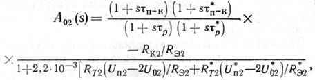
![]()
where ![]() is
the oscillation amplitude of the infrasound frequency at the output of ASF, in
Volts; UR1 is the constant voltage at the load DS, in Volts;
is
the oscillation amplitude of the infrasound frequency at the output of ASF, in
Volts; UR1 is the constant voltage at the load DS, in Volts; ![]() is the modulus of the total dynamic
resistance of the load of DR at the infrasound frequency, in Ohms;
is the modulus of the total dynamic
resistance of the load of DR at the infrasound frequency, in Ohms; ![]() is the sensitivity function that connects
the amplification of the ASF with the common negative feedback coupling to the
change in amplification of its forward transfer at the frequency of the useful
signal. Since the loop gain of the common negative feedback coupling of ASF
turns by phase ±p/2 between the frequency of the dominant
pole of the common negative feedback coupling and the frequency
is the sensitivity function that connects
the amplification of the ASF with the common negative feedback coupling to the
change in amplification of its forward transfer at the frequency of the useful
signal. Since the loop gain of the common negative feedback coupling of ASF
turns by phase ±p/2 between the frequency of the dominant
pole of the common negative feedback coupling and the frequency ![]() , then the parasite amplitude modulation
becomes the frequency modulation as a result of the amplitude-phase conversion
(APC) [19], i.e. one can observe the distortions of BIMF type at both low and
high sound frequencies at the output of ASF with the common negative feedback
coupling.
, then the parasite amplitude modulation
becomes the frequency modulation as a result of the amplitude-phase conversion
(APC) [19], i.e. one can observe the distortions of BIMF type at both low and
high sound frequencies at the output of ASF with the common negative feedback
coupling.
Distortions of the envelope function.
Distortions of the envelope function in the experimental ASF (see Fig.1) also
appear in DS because of non-linear coupling of the transfer characteristic of
the useful signal, which has a form of the amplitude-modulated oscillations,
with the signal representing the envelope function of these oscillations. The
latter is formed as a result of non-linear conversion of the
amplitude-modulated oscillations on the transfer characteristic of DR (see
Fig.2) at the frequencies ![]() .
.
If we recognize the fact that the envelope
function of the voice or musical signal has a finite frequency spectrum, then
the amplitude of the modulated oscillations can as well be less than the
amplitude of the signal representing the envelope function (taking into account
the loop gain of ASF dies at the frequency ![]() )[15].
)[15].
Therefore, the error signal of the common
negative feedback coupling is being formed between the two inputs of DS; this
error signal has a dominant infrasound oscillation component, which is a
derivative of the envelope function of the useful signal. Thereby, if the
amplitude of the signal doesn’t leave the linear part of the transfer
characteristic of DS, then the infrasound intermodulation distortions of BIMA
type, defined in [18] as envelope function distortions, are formed in DS.
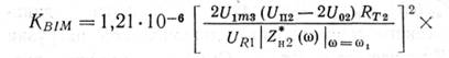
Taking into consideration the common
negative feedback coupling, the distortion coefficient of the envelope function
of ASF can be determined according to the following formula [15]:
![]()
where ![]() is
the maximum value of the amplitude of the modulated signal at the output of
ASF, in V;
is
the maximum value of the amplitude of the modulated signal at the output of
ASF, in V; ![]() is the modulus of the total dynamic
resistance of the load of DS at the frequency
is the modulus of the total dynamic
resistance of the load of DS at the frequency ![]() in Ohms; S(w) is the sensitivity function that
connects the amplification of the ASF with the common negative feedback
coupling with the change in amplification of ASF forward transfer at the
frequency of the spectrum of the modulated oscillations.
in Ohms; S(w) is the sensitivity function that
connects the amplification of the ASF with the common negative feedback
coupling with the change in amplification of ASF forward transfer at the
frequency of the spectrum of the modulated oscillations.
As it was in prior cases, in the discussed
instance one can observe the conversion of BIMA into BIMF, therefore, the
distortions of the envelope function are being transformed into distortions of
the instantaneous carrier frequency of the useful signal as a result of APC.
The results of the
experiment.
During the experimental studies of the
effects performed on the prototype device (see Fig.3), it turned out that the
most convincing result was the observation of the linear thermal
distortions on the transistor VT4, since there are no other possibilities for
the appearance of other types of distortions in the given frequency window. We
measured the AFC and the transfer reaction of the error signal in the summing
junction of the amplifier. It was determined that the error signal in the
summing junction of the amplifier grows from 60 to 20 when a sine wave voltage
is applied at the input of that amplifier. The relative gain of the signal was
7 dB. The measurements were carried out on the middle sound frequencies, where
we found another frequency window from 2.8 – 1.5 kHz with a relative gain of
the error signal 5 dB. This phenomenon can be explained by the existence of the
local heating-up zones in the crystal that, as it is well known, are the reason
for the formation of the secondary breakdown region in transistors.
Conclusion
It has been revealed that practically
every transistor in the amplifier is a source of the thermal distortions in the
low sound frequency region. The application of the composite signal at the
input of ASF in this case leads to the transformation of these distortions into
infrasound intermodulation distortions, known as Bass Intermodulation (BIM)
[3].
Thermal distortions appear when the
instantaneous signal interferes with the thermosensitive
parameters of the transistor – current amplification coefficient and the
base-emitter voltage, due to thermoelectric conversion in transistors [15].
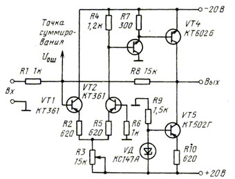
Fig.3. The principle electric circuit of
the ASF prototype that has been used for the measurements of thermal distortions.
The current gain of the output stage (see
Fig.1) can change by 200-300% due to the change of the dissipated power on the
collector of the transistors during the transmission of the real (non-stationary)
signal. This leads to the change of the voltage gain of that stage. The rate of
this change is low, being limited by the thermal time constants junction-case
of the transistor. However, even this slow change affects the distortion of the
signal envelope function and it is significant for perception of the signal.
The most significant parameter in the
driver stage and its dynamical load is the thermal sensitivity of the
base-emitter voltage of the transistors. As a result of the conversion of the
stage output voltage into instantaneously dissipated power on the collector of
the transistor, then into the temperature of p-n junction, and then into the
change of the base-emitter voltage, the non-linear thermoelectric feedback
coupling is formed, which causes the reduction of the gain of that stage and
the increase of the non-linear distortions in the low sound frequency region.
The differential stage, in spite of the
low signal value at the output, also shows the noticeable influence of the
thermoelectric feedback coupling, which is a linear one in this case, and
moreover, it is positive.
Thermal distortions can be detected at the
output of ASF with a common negative feedback coupling (see Fig.1). One can
observe [15]:
·
Harmonic distortions in the low sound frequency region
(under 100 Hz);
·
Infrasound intermodulation distortions of BIMA and BIM
type;
·
Envelope function distortions, produced in the output
and differential stages; in the latter case
·
due to the transfer of the significant error voltage
back to its input by the negative feedback loop.
The infrasound intermodulation distortions
and envelope function distortions, converted into the parasite frequency
modulation (BIMF) due to AFC, cannot be controlled in the household ASF. At the
same time, it is known [7] that even the smallest values (approximately 0.06%)
of the frequency modulation in the composite signal are audible. This
subjective difference in perception of different ASF with similar traditionally
controlled parameters can apparently be explained by the distinct values of the
BIM type distortions.
Reference:
1. Вахandall P. J. Audible amplifier distortions not a mystery, Wireless World,
1977,83, N11, pp. 63-66.
2. Bespalov, Pikersgil А., The quality of sound and characteristics
of AMSF, Radio, 1986, N1, pp. Е6-57 (in Russian).
3. Мoller Н. Multidimensional Audio: Part 3., JAES,
1979, 27, N 7/8, pp. 562-567.
4. Seashure H.
An objective analysis of artistic singing. - Objective Analysis of Musical
Performance. - Studies the Psychology of Music.
5. Tsviker E., Feldkeller R., Ear as an information receiver. -
6. Method of measurement of spread fluctiations in sound recording and reproduction equipment.
IEC Publication 3f6,
7. Saka I H.
Perceptibility of Wow and Flutter., JAES,1970,18, N*3, p. 290-298.
8. Household tape recorders. General
technical conditions. ГОСТ 24*63-81 (in Russian).
9. Grem J., Toby
J.,Hulsman M., Design and application of operational
amplifiers, Moscow.: Mir (World), 1974, pp. 64-77 (reference made to the pages
in Russian translation).
10. Laue В.A.
Family of amplifiers (Part 3), Hi-FiNews, 1970, N 9,
pp.1236-1239.
11. Haas G.C. Design Factors and Considerationsin Full complementary Symmetry Audio Power
Amplifier, JAES, 1968, 16, N 3, pp.
321-326.
12. Paul R., Transistors, Moscow.: Sovetskoye Radio (Soviet Radio), 1973, p.
492.
13. Оррегmann W. Probleme bei eisenlosen End-stufen. - Funkschau,
1968, H.16, ss. 551-552.
14. Fishtein A.M., Distortions in linear
amplifiers caused by the AC component of transistor p-n junction temperature,
Collection of Works of IPSB (Institute of Physics of Siberian Branch of Academy of
Sciences of U.S.S.R., Krasnoyarsk), 1977, issue 68, series Physics, pp.1-23.
15. Likhnitsky A.M., On the source of
distortions: amplifiers in the low sound frequency region, in the book
“Experience, results, problems: increase of competitive ability of radio
electronics equipment,” Collection of articles, issue 3,
16. Titse, W.,
and Shenk, K., Semiconductor Circuit Design,
17. Dе Магinis J.U., How Valid is the FTC
Preconditioning Rule, Audio, 1975, 59, N3, pp. 30, 32, 34, 50.
18. Curl J., Omitted Factors in Audio
Design, Audio, 1979, 63, N9, pp. 22-26.
19. Krylov, G.M.
(editor), Amplitude-phase conversion,
20. Landee, R.,
21. Handbook, N.N. Goryunova,
(editor), Semiconductor devices: transistors,
22. Ноlman T., Phonograph Preamplifier Design
Criteria, An Update, JAES, 1980, 28, N5, pp. 325-330.
23. Оtala M., Ensonaa R.,
Transient intermodulation Distortion in Commercial Audio Amplifier, JAES, 22 ,
N4, p. 224.
24. Cherry Е.М., Amplitude and Phase of Intermodulation
Distortion, JAES, 1983, 31, N5, pp. 238-304.